
I think I found an error in the E&E sample questions. I posted my understanding and proposed solution below. If I am mistaken, please let me know.
For problem 10 on page 42-5, the following solution is given:
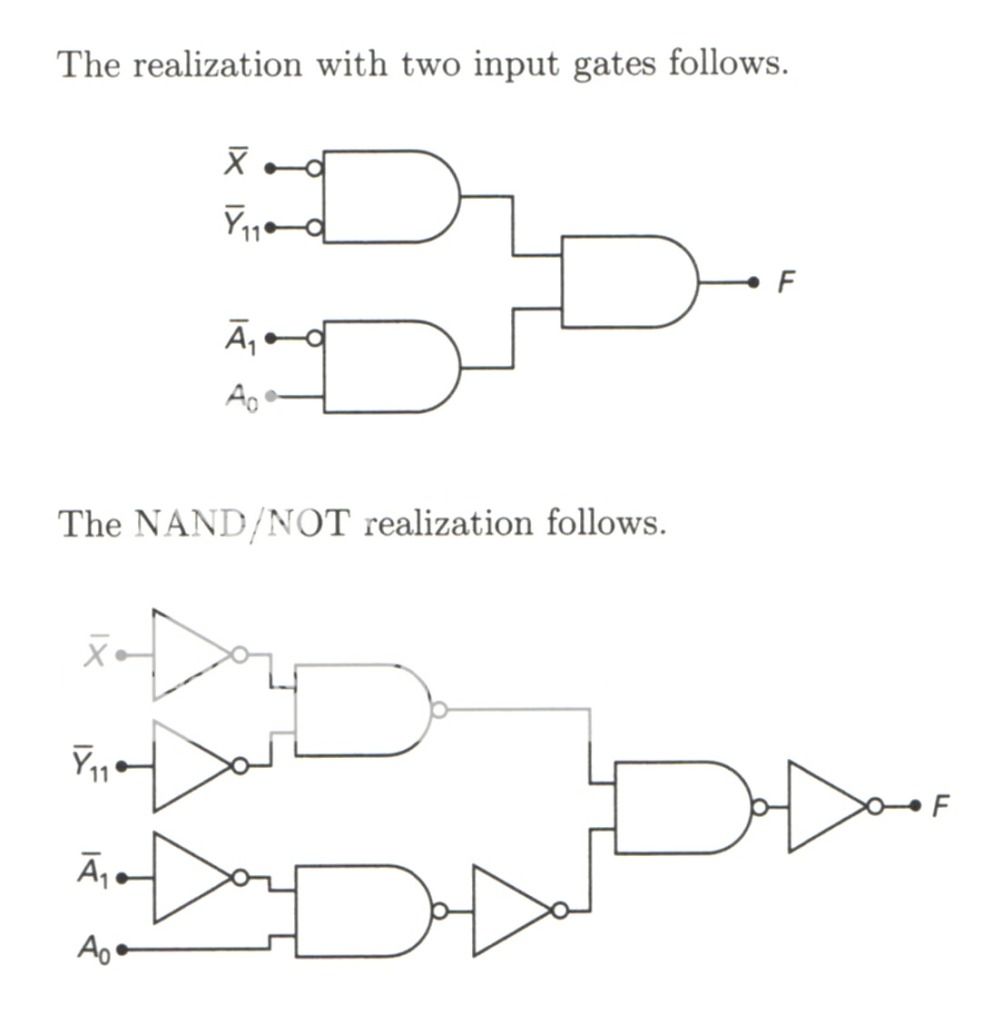
The NAND/NOT realization is incorrect. There should be an additional NOT gate between the two NAND gates that have no gates between them, as follows:
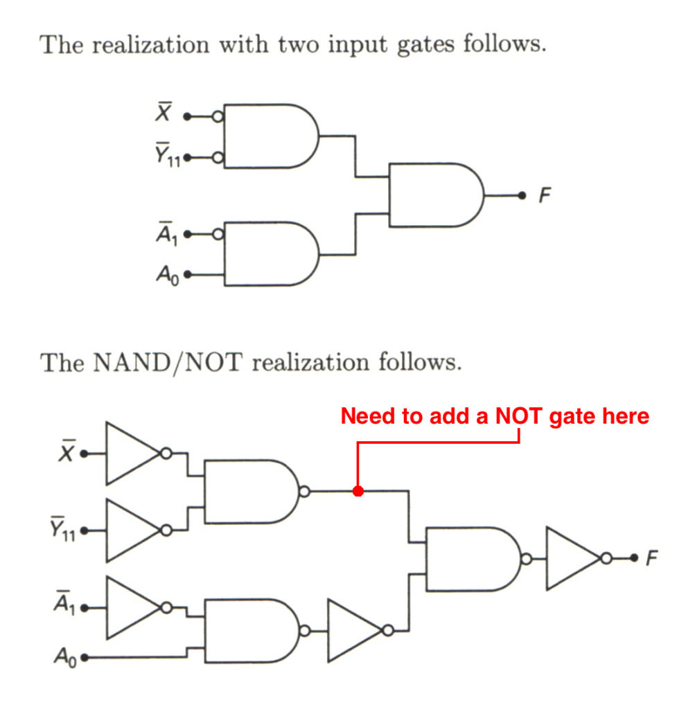
For problem 10 on page 42-5, the following solution is given:
The NAND/NOT realization is incorrect. There should be an additional NOT gate between the two NAND gates that have no gates between them, as follows:

